technology
Step PCB | frame technology | exposed inner layers | 3D | printed circuit board | multilayer assembly
Step and frame PCBs - differences & application
Frame and Step Technology are similar yet fundamentally different printed circuit board (PCB) technologies. They form a kind of "2.5D technology," where the typically two-dimensional PCB surfaces are modified with elevations or recesses. The primary difference between frame and step PCBs is whether copper structures are required on the outer layers or if they only exist internally.


Frame Technology

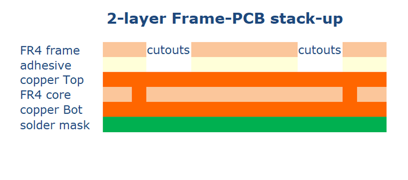
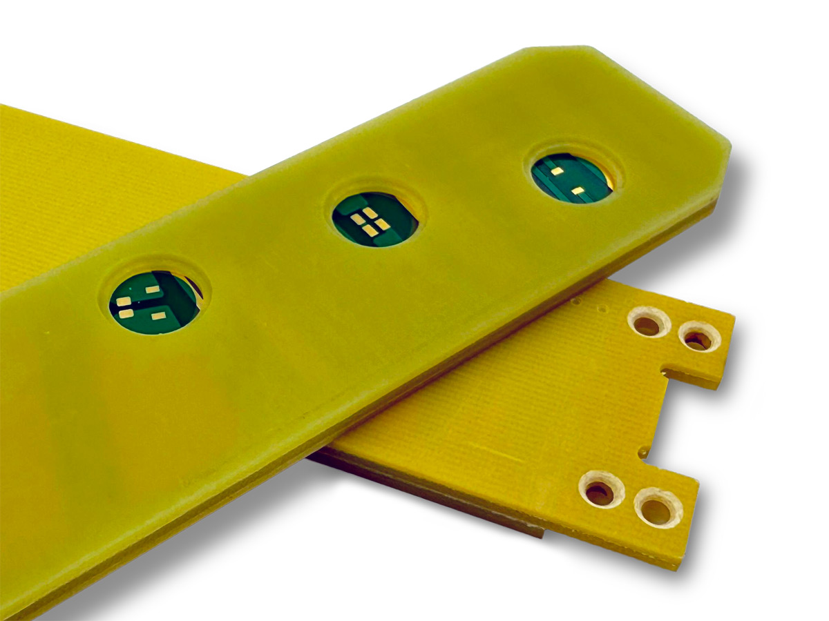
In Frame Technology, one or both sides of the PCB are laminated with FR4 parts using 3M adhesive or no-flow prepreg (which is more expensive). These FR4 frames usually provide mechanical protection. In some cases, the cutouts serve as "pockets" for encapsulating mounted components.
Advantages of Frame Technology:
- Cost-effective process
- Possible on both sides, with varying thicknesses
- Special mechanical processes are possible
- Contactable, internal structures
- High-layer count multilayers can be cost-effectively combined with frames
Disadvantages of Frame Technology:
- The outer side of the frame has no copper
- No conductive connection from the outside to the inner layer
- 3M adhesive is less stable than prepreg bonding
- Placement limitations (must be adjacent to the contour)
- Frame edges may show slight resin leakage or minimal resin retraction
Step Technology

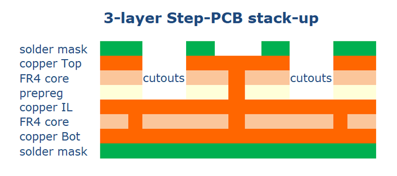
In Step Technology, complete multilayer PCBs are produced using laminate technology. Laminate technology refers to a process where the outer layers are not pressed as foil but are instead complete two-layer cores. However, the areas that will later be exposed are deep-milled from the back of the core and cut out in the prepreg before pressing. After completing the multilayer, these areas are deep-milled so that the unbonded parts can be removed, and the inner layers are exposed.
Advantages of Step Technology:
- Possible to expose on both sides, with varying thicknesses
- Copper structures on both the inside and outside
- Stable prepreg bonding
- Flexible placement of the exposed areas
- Special mechanical processes are possible
- Contactable, internal structures
Disadvantages of Step Technology:
- Complex, expensive process
"Frame PCBs" are a type of 2.5D technology, where non-plated FR4 parts are glued onto the PCB.
Applications include side protection for specific components. Additionally, open frame cutouts allow for the use of additional potting materials.
After the PCB fabrication, milled frame parts (usually FR4) are precisely glued onto one or both sides using 3M adhesive.
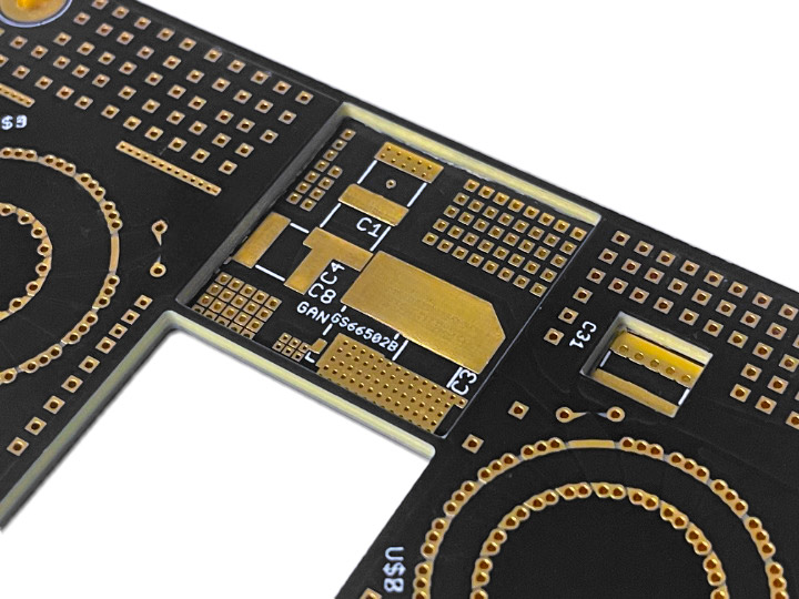
"Step PCBs" are a 2.5D technology, where different plated-through areas have varying height levels.
Step PCBs can have plated through-holes (PTH) and copper structures on all levels (more expensive). Frame PCBs use glued non-plated parts, making them a more cost-effective alternative.
Advantages:, Cost-effective, different thicknesses possible on both sides, complex multilayers can be expanded using frames at a low cost
Disadvantages: No plated through-holes or copper structures on the frame, 3M adhesive is less stable than prepreg, requires precise contour alignment
Advantages: Plated through-holes and copper structures are possible on all stepped levels, stable prepreg bonding, internal and external copper layers possible
Disadvantage: Complex and costly manufacturing process

since 2021
- CO2 neutral through compensation
- Circuit boards – green on the outside, also on the inside

- Expertise through active exchange
- Expertise through training and further education
- ISO 9001:2015 Quality Management
- ISO 14001:2015 Environmental Management

- UL for rigid FR4 PCBs
- UL for flexible circuit boards
- UL for aluminum IMS boards


