Chemical Gold | HAL | ENIG | Printed Circuit Boards | PCB | Surfaces
8 PCB surfaces in comparison - electroless gold (ENIG) vs. HAL (Hot Air Leveling) & Co.
Printed circuit boards can be coated with various end surfaces (also known as “surface finishes”) to improve the smooth processing of different components, general solderability, reliability and durability. The individual surface finishes are explained in more detail in the surface finish overview table.
| Abbreviation | HAL | HAL leaded | CSN | IS | OSP | ENIG | ENEPIG | Connector gold |
|---|---|---|---|---|---|---|---|---|
| Description | HAL - lead free | HAL leaded | Immersion tin | Immersion silver | Organic Surface Passivation | Electroless Nickel-Gold | Electroless Nickel-Palladium-Gold | Electroplated Nickel-Gold |
| Layer thickness | 15 - 50µm | 15 - 50µm | 0,8 - 1,2µm | 0,2 - 0,4µm | 0,2 - 0,6µm | Ni: 3 - 6µm / Au: 0,05 - 0,125µm | Ni: 3 - 6µm / Pd: 0,05 - 0,15µm / Au: 0,025µm | Ni: >4µm / Au: 0,5 - 3µm |
| Solderability | ++ | +++ | ++ | ++ | + | +++ | +++ | o |
| Multiple Soldering | ++ | ++ | - | + | - | +++ | +++ | - - |
| Al-Wire-Bonding | - - | - - | - - | + | - - | ++ | ++ | - - - |
| Au-Wire-Bonding | - - | - - | - - | - - | - - | - - | +++ | - - - |
| Fine-Pitch | - | - | +++ | +++ | +++ | +++ | +++ | - - - |
| High frequency | o | o | +++ | +++ | ++ | o | o | o |
| Pressfit | ++ | ++ | o | o | - - - | o | o | o |
| Key-Press (Keyboards) | - - | - - | - - - | - - - | - | + | + | +++ |
| Corrosion Resistance | ++ | ++ | - - | - - | - | ++ | ++ | +++ |
| Refreshable | ja | ja | ja | nein | ja | nein | nein | nein |
| Shelf life | + | + | - | o | o | ++ | ++ | +++ |
| Cost | $ | $ | $ | $ | o | $$ | $$$ | $$$$$ |
| RoHS-compliant | ja | nein | ja | ja | ja | ja | ja | ja |
| Availability | ++ | o | ++ | - | o | ++ | + | + |
Immersion Tin (CSN)
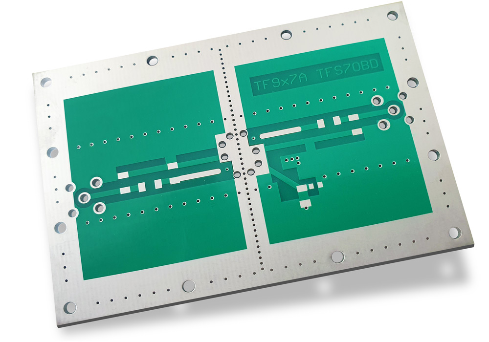
Immersion Tin is widely used in Europe due to its cost-efficiency and fast processing. In this method, PCBs are typically submerged in tin baths using a basket technique. Over time, the tin deposits on the exposed copper pads. It is crucial to ensure proper circulation of the bath so that the tin-containing solution can flow effectively between the PCBs. However, it should be noted that this process slows down over time. Once a layer thickness of approximately 1.2 µm is reached, little to no additional tin is deposited, regardless of how long the PCB remains in the tin bath.
The typical thickness for immersion tin ranges from 0.8 µm to 1.2 µm. A minimum of 1.0 µm of tin is recommended to optimize shelf life and ensure the possibility of a second reflow process. However, immersion tin is not suitable for more than two soldering cycles.
- Good solderability due to the pure tin surface.
- Flat surface, making it ideal for SMD components.
- RoHS-compliant, as it is lead-free.
- Cost-effective compared to other surface finishes.
- Prone to tin whisker formation, which can cause short circuits.
- Limited shelf life due to oxidation (maximum of 6 months).
- Sensitive to fingerprints and environmental conditions, which can lead to corrosion.
- Only moderately suitable for multiple reflow cycles.
Electroless Nickel Immersion Gold (ENIG)
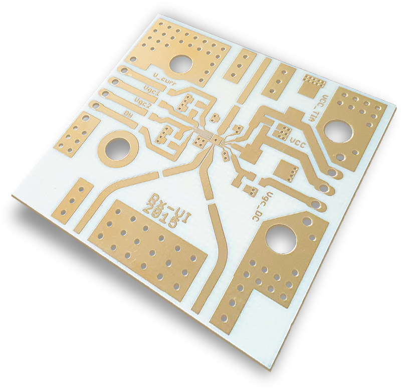
Electroless Nickel Immersion Gold is considered the best surface finish for storage and processing. Additionally, ENIG is compatible with aluminum wire ultrasonic (US) wedge bonding. However, for bonding with gold or copper wires (thermosonic (TS) ball/wedge bonding), ENIG is unsuitable; ENEPIG should be used instead.
According to IPC-4552, the surface should have a minimum of >3 µm nickel and >0.05 µm immersion gold to ensure optimal storage. For flexible PCBs, thinner layers are often deliberately used because nickel tends to be porous and can crack under bending.
- Excellent solderability, even after extended storage.
- Extremely flat surface, ideal for SMD components and BGAs.
- Optimal surface for multiple soldering processes.
- High-quality surface, suitable for fine-line structures.
- Corrosion-resistant and offers very long shelf life (12 months or more).
- Versatile, usable for various applications, including contact areas (e.g., keypads).
- Higher costs compared to other surface finishes.
- Risk of the "Black Pad" phenomenon, where a poor nickel-phosphorous layer can compromise reliability.
- More complex manufacturing process.
- The presence of the nickel layer can make it unsuitable for high-frequency (HF) or medical applications.
Immersion Silver (IS)
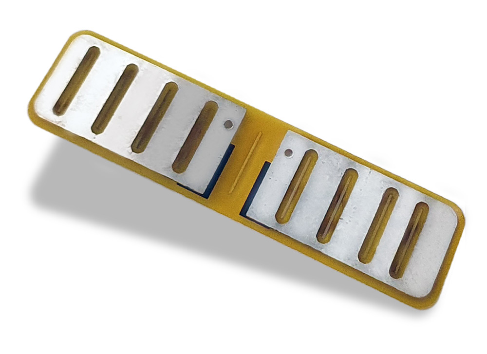
Immersion silver is a relatively new process that gained widespread adoption in the early 2000s. At the same time, leaded soldering, often done using the HAL process, was banned. Immersion silver emerged as a lead-free, RoHS-compliant alternative, competing with the also relatively new immersion tin process.
While immersion tin became more popular in Europe, immersion silver has found broader use in the United States.
- Good solderability.
- Flat surface, suitable for fine structures.
- More cost-effective than ENIG.
- Excellent electrical conductivity, ideal for HF applications due to the absence of a nickel layer.
- Widespread acceptance and use in the U.S.
- Prone to tarnishing and oxidation, especially in humid environments.
- Shorter shelf life compared to ENIG (up to 6 months).
- Sensitive to environmental factors (e.g., sulfur exposure).
- Limited use in Europe and Asia, resulting in lower availability (chemically tin dominates in Europe, ENIG in Asia).
Leaded Hot Air Solder Leveling (HAL Leaded / HASL - Hot Air Solder Leveling)
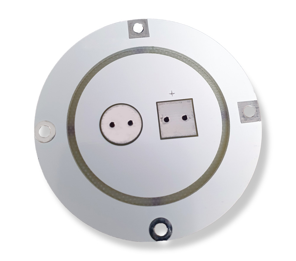
In the hot air process, PCBs are first completely coated with flux and then immersed in a hot, molten tin bath. When withdrawn from the tin kettle, the PCB passes between two opposing air knives, which use high-pressure air to blow off the excess, still-soft tin. This process results in uneven tin layers on the solder pads, which can cause ripples, especially on large, hole-free surfaces. Lead-based soldering is now largely banned in Europe and the U.S., and it is only used by a few PCB manufacturers, typically those producing for military applications. The process was fast, cost-effective, reliable, but also hazardous.
Due to the ban on leaded solder, materials capable of withstanding higher thermal stresses had to be developed, leading to the emergence of many new high-Tg materials for lead-free soldering in the early 2000s.
- Low eutectic point, minimizing stress on the PCB.
- Fast and cost-effective process.
- Good solderability for through-hole technology (THT) and leaded components.
- Long shelf life (up to 12 months).
- Limited availability due to widespread prohibition.
- Uneven surface, unsuitable for SMD components.
- Not suitable for large copper areas (tin cannot be fully removed by air knives).
- Risk of solder balls, which can cause short circuits.
- Not ideal for fine-pitch designs and densely populated PCBs.
Lead-Free Hot Air Solder Leveling (HAL Lead-Free / HASL - Hot Air Solder Leveling)
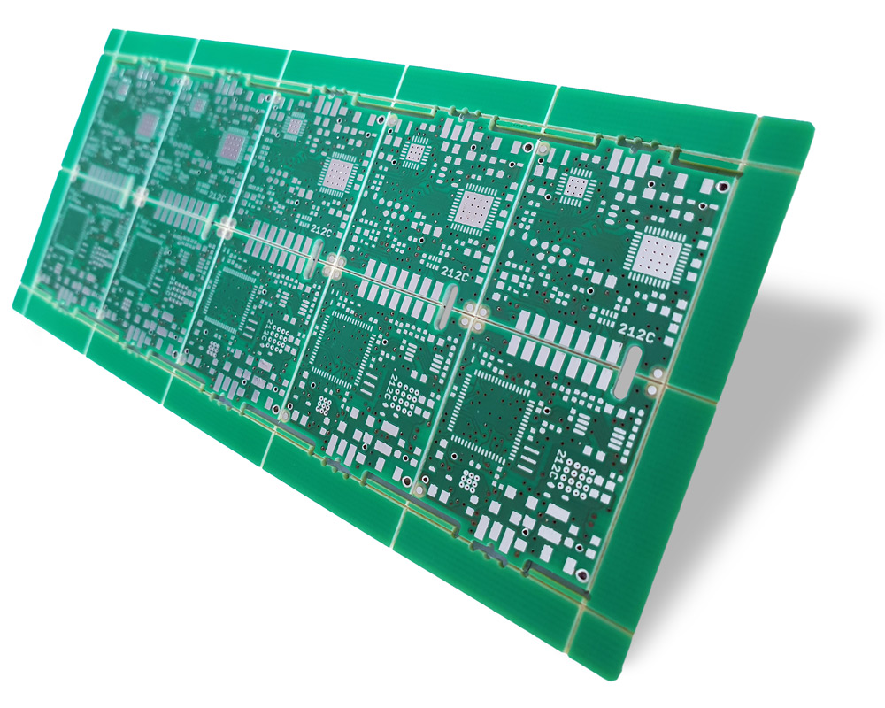
Lead-free HAL operates identically to the previously described leaded HAL process, but significantly higher temperatures are required. Pure tin requires temperatures around 275°C in the solder pot, which puts significant thermal stress on the PCB. High-layer-count multilayers or SBU (Sequential Build-Up) structures should therefore ideally not be processed using this method, as the high temperatures could cause barrel cracks.
Since such PCBs are typically equipped with fine-pitch components and BGAs, ENIG (Electroless Nickel Immersion Gold) is recommended as the final surface finish for these applications.
- Cost-effective and widely used surface finish.
- Durable and robust.
- Good solderability for through-hole technology (THT) and leaded components due to the larger tin deposit.
- Long shelf life (up to 12 months).
- Uneven surface, less suitable for SMD components.
- Risk of solder balls, which can cause short circuits.
- Not ideal for fine-pitch and densely populated PCBs.
- High thermal shock to the PCB during the process.
OSP (Organic Solderability Preservative)
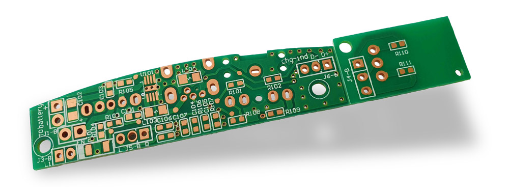
OSP surfaces are very cost-effective and can be applied quickly to PCBs. However, due to their limited resistance and shelf life, this finish is rarely used in high-end medical, automotive, IT, or industrial electronics, and is mostly applied in low-cost mass-market and consumer electronics.
In Europe, OSP is not commonly used, whereas in China, it is a widespread alternative for inexpensive PCBs.
- Very cost-effective.
- Environmentally friendly and RoHS-compliant.
- Flat surface, ideal for SMD components.
- Relatively short shelf life (3 to 6 months), as the organic layer degrades over time.
- Not suitable for multiple soldering cycles.
- No protection against environmental factors (e.g., moisture).
- Low mechanical protection (e.g., against scratches).
- Limited use in Europe.
Selective Electroless Gold (Hard Gold)
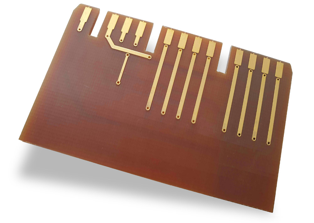
Hard gold is typically applied as a supplementary surface finish on PCBs and is rarely used for large areas that experience mechanical stress (e.g., plug-in contacts). The high costs involved and the required process are the main reasons for this. Hard gold surfaces need an electrical connection between the areas to be gold-plated and the edge of the production panel so that they can be contacted and galvanically connected.
This is the only way to achieve gold deposits of over 0.5 µm (the common minimum) up to the required 3 µm in some cases.
- Very robust and durable, ideal for mechanically stressed contact areas (e.g., connectors, keypads).
- High corrosion resistance.
- Long shelf life.
- Very expensive compared to other surface finishes.
- Harder finish, making it less suitable for soldering, and therefore mostly used for specific areas of the PCB.
- High material consumption (gold), which can increase environmental impact.
- The gold-plated areas must be additionally contacted via traces.
- Visible remnants of the galvanic bus connection, which can be removed with a more complex etch-back process.
Electroless Nickel / Palladium / Gold (ENEPIG)
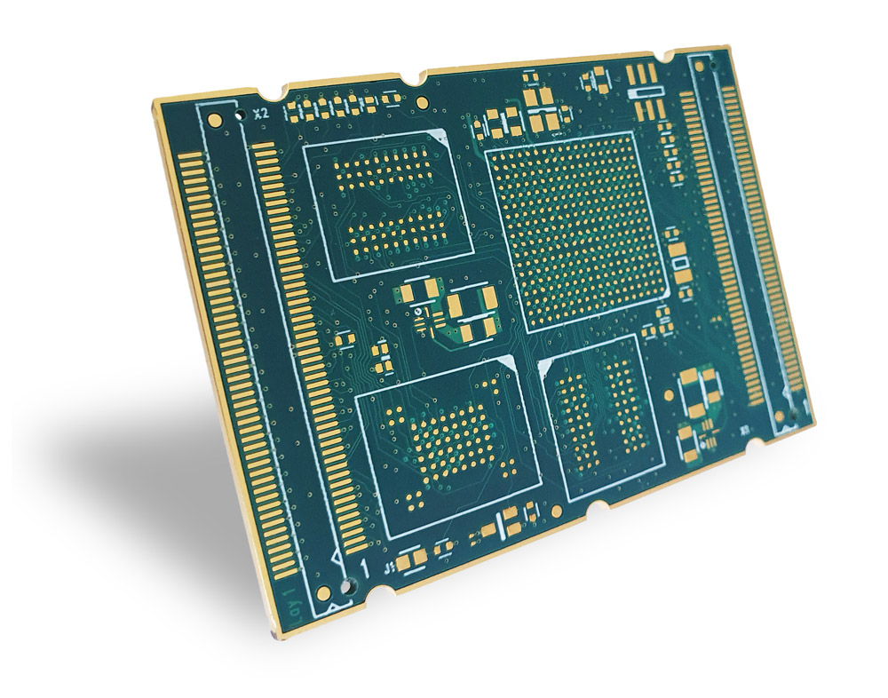
ENEPIG is a relatively new surface finish that is used in conjunction with ENIG. The main advantage of ENEPIG is that it allows for thermal bonding with both copper and gold wires. Previously, a more expensive and thicker soft gold surface was required for this process, but ENEPIG has largely replaced it.
The IPC 4556 standard applies here as well, specifying 3 to 6 µm of nickel under a thin 0.05 to 0.15 µm palladium layer, followed by a thin 0.025 µm gold layer.
- Very high solderability and excellent electrical properties.
- Provides protection against "Black Pad" issues that can occur with ENIG.
- Suitable for fine structures and various applications.
- Thermal bonding is possible.
- Very high cost in prototype manufacturing.
- Complex manufacturing process.
- Less widely available, which can result in longer lead times.
ENIG: Smooth & corrosion-resistant. HASL: Cost-effective & robust. Immersion Tin: Smooth but prone to oxidation & not ideal for long-term storage.
- ENIG (Electroless Nickel Immersion Gold): Nickel layer with a thin gold coating (~0.05µm), offering high corrosion resistance & excellent planarity.
- HASL (Hot Air Solder Leveling): Molten solder layer, leveled with hot air, provides a good solder depot but results in a less even surface.
- Immersion Tin: Thin chemical tin layer (~1µm), very smooth but oxidation-prone.
ENIG is durable & corrosion-resistant, HASL is cost-effective & robust, while immersion tin offers a smooth surface for fine traces but is oxidation-sensitive.
- ENIG: Highly planar, corrosion-resistant, long shelf life but more expensive.
- HASL: Cost-effective, strong solder joints due to its own solder depot, but uneven surface.
- Immersion Tin: Affordable, smooth surface suitable for fine-pitch structures, but oxidizes quickly
ENIG & Immersion Tin are ideal for sensitive & fine-pitch components, while HASL is better for robust solder joints.
- ENIG: Best choice for sensitive components, smooth & oxidation-free surface, optimal for fine-pitch designs.
- Immersion Tin: Suitable for fine structures but has limited shelf life and is less reliable for multiple soldering cycles.
- HASL: Suitable for standard PCBs but can be problematic for fine structures, though it has good storage stability and allows multiple soldering processes.
ENIG & Immersion Tin offer very good solderability; Immersion Tin is ideal for SMT, while HASL is well-suited for THT but has an uneven surface.
- ENIG: Excellent solderability (even for multiple reflows), long-lasting connections, but requires specific soldering parameters.
- HASL: Good solderability, especially for THT components, but uneven surface. Allows multiple soldering cycles.
- Immersion Tin: Good for SMT, but oxidation-prone and not optimal for multiple soldering processes.
ENIG lasts the longest (sometimes over a year), HASL has medium durability (up to 1 year), and Immersion Tin oxidizes quickly (up to 6 months).
- ENIG: Best durability, resists corrosion & environmental influences, easy to clean.
- HASL: Medium durability, oxidizes faster than ENIG.
- Immersion Tin: Shortest shelf life, highly susceptible to oxidation and fingerprints.
ENIG is expensive, HASL has an uneven surface, and Immersion Tin is oxidation-sensitive & has a short shelf life. Each method has its specific application limits.
- ENIG: High cost, complex manufacturing process, risk of "Black Pad" defects.
- HASL: Uneven surface, not suitable for fine structures.
- Immersion Tin: Short shelf life, prone to oxidation.
ENIG is ideal for high-end PCBs, HASL for standard applications, and Immersion Tin for fine-pitch PCBs with cost constraints.
- ENIG: Ideal for high-end PCBs & sensitive components.
- HASL: Good for standard PCBs, cost-effective & robust.
- Immersion Tin: Suitable for fine-pitch structures but prone to oxidation
HASL is the most environmentally friendly, while ENIG & Immersion Tin require more chemicals, with the latter often containing problematic additives.
- HASL: More eco-friendly due to lower chemical consumption.
- ENIG: Requires nickel & gold, making it resource-intensive.
- Immersion Tin: Often contains additives that can be environmentally harmful.
HASL is the most cost-effective option, Immersion Tin is moderately priced, while ENIG is the most expensive due to material & process costs.
- ENIG: Most expensive method due to gold & nickel plating and complex process.
- HASL: Cheapest option, ideal for standard PCBs & high-volume production.
- Immersion Tin: Mid-range cost, but offers good planarity for SMT.
Yes, different surface finishes can be combined to leverage their respective advantages for specific PCB areas. However, this can lead to high costs, as additional manual processing steps (masking/protection) are usually required.


