Aluminum PCBs (MCPCB) | Thermal Management & Cooling | High Reliability | Application Areas | Manufacturing Technology
Aluminum PCBs – Efficient Heat Dissipation for Robust Electronics
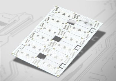
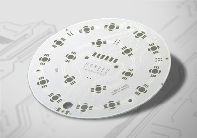
Aluminium-PCBs, or IMS printed circuits („Insulated Metal Substrate“) offer cost-efficient solution to manage the heat for high-performance LED-technology or transistor-electronics . Today, IMS-PCBs can exceed 1 layer and aluminium can be integrated in standard double-sided or even multilayer printed circuit boards.

The keyword „hot-spots“ triggers several fears in a layout designer's ear. Top of the list is that standard FR4 PCBs will not do the trick anymore but a special materials solution is needed. If hot-spots are ignored this may cause severe damage and reliability issued for the final electronics assembly group. Reduced lifetime of components due to persisting heat are only one concern. In extreme cases hot-spots can lead to de-soldering of the component and the product fails in the field quickly. Aluminium IMS printed circuits help distributing heat from hot-spots. This reduces accumulated heat close to the component and instead of punctual hot-spots the whole printed circuit board warms up homogeneously with lower temperatures.
The distribution of heat by conducting it into the PCB is nothing else than an effective passive cooling mechanism of the components. By adding fans or other cooling components to the PCB this can be the first step of a more powerful active cooling. It is very common that aluminium IMS PCBs are cooled from the backside of the board. The supply of coldness on the backside works the same way like heat is dissipated from the components. Coldness is well distributed from the back and reaches the heat emitting components and cools them down. Heat conductance works both ways.
A commonly misunderstood topic is the „heat conductance of aluminium“. For most common alloys heat conductance of aluminium is 234W/mK. This is slightly less than for example copper, which may also be used for heat management in PCBs at slightly higher costs. Silver, with around 100 times the raw material price of aluminium is not an option. Latest developments in nano-technology come up with so called graphene which is extremely good in conducting heat, but does so only in z-direction. Therefore, graphene is not useful to conduct heat through a carrier but only when added as foil on areas during assembly. It should be noted that graphene is a very expensive product as well. All this explains why aluminium is the dominant material in IMS PCBs and heat management in electronics.
When categorizing aluminium IMS materials it is not the heat conductance of the aluminium that is of any concern (it is mostly given by the element/alloy itself). What is of concern, is the isolation area between the copper cladding and the aluminium carrier. The higher the heat conductance of this material, the better heat can dissipate from the copper (components) through the insulation into the aluminium, which will then spread it out over the PCB area. The thickness of this insolation influences the performance, too. It commonly ranges at 75µm to 100µm.
| material | heat conductance [W/mK] |
|---|---|
| graphene | ~5000 |
| diamond | ~2300 |
| cilver | 429 |
| copper | 398 |
| aluminium | 234 |
| heat-conducting epoxy | 1,0...3,0 (somtimes up to 8,0 and higher) |
| normal epoxy | 0,38 |
| water | 0,6 |
| air | 0,02 |
| vacuum | 0 |
While single-sided aluminium PCBs are commonly clear in the required design, the enquiry of double- and multilayer IMS-PCBs may lead to misunderstandings concerning the required stack-up during the quotation process. In these cases, the aluminium layer can be accessible attached on the outside or it can be integrated into the stack itself. To avoid confusion, having aluminium on the outside of a PCB should therefore be referred to as "aluminium carrier" PCB, while having aluminium inside the stack should be called "aluminium core" PCB.
Design tips for aluminium-IMS printed circuit boards
As normal copper cladding is laminated onto the aluminium with an insulation in between, there are no changes or restrictions in terms trace width or distance compared to standard printed circuit boards. However, one has to pay attention to via-drill distances in between each other. In order to insulate vias or component drills, the hole has to be drilled larger first and then it is filled with an insulating paste. This process applies to single-sided aluminium carrier PCBs that require THT components as well. Otherwise the component or the drill will short over the aluminium carrier/core. There are also heat-conducting filler-pastes available that increase heat dissipation.
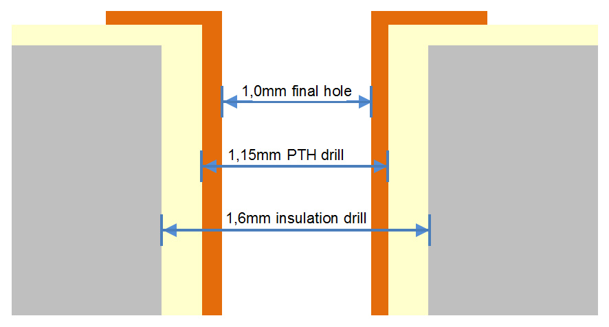
A plated through hole with a final diameter of 1,0mm according to original layout will usually be drilled with a surplus of 0,15mm, resulting in a 1,15 drill bit. With this surplus it is assured that the copper wall and the surface finish can be applied without resulting in a smaller hole than the required 1,0mm. If insulation from the aluminium is required, another 0,45mm are added to the drill size to drill a isolation hole into the aluminium core first. These additional 0,45mm are there to make sure that the later plating drill does not hit the aluminium, which would result in a short during the through hole plating process. The following picture explains the different drill sizes for aluminium core PCBs:

- drill in original layout (= final drill size): 1,00mm
- surplus of 0,15mm for though-hole-plating: 1,15mm
- surplus of 0,45mm for insulation: 1,60mm
Furthermore, please note that the smallest possible drill bit for any insulation drill through aluminium is 1,0mm. Smaller diameters cannot be drilled into aluminium. Even 0,3mm drills must therefore be pre-drilled into the aluminium with a 1,0mm drill bit instead of the theoretical 0,9mm (drill bit +0,6mm).
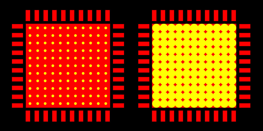
Due to these procedures, widely used thermal vias may be counterproductive or even impossible in aluminium-core PCBs. Large areas of well conducting aluminium have to be removed for thermal vias - far more than later visible from the outside. Depending on the drill distance this may even lead to the break-off of large aluminium parts when thermal-via insulation drills begin to overlap. This area could not be filled and insulated with paste anymore and the result in heat conductance would likely be worse than leaving the aluminium untouched underneath anyway.

When designing IMS PCBs it may therefore be smarter to remove thermal vias from the layout and instead rely on the aluminium inside the carrier for heat conduction.
Soldering of aluminium IMS printed circuits

Solderin aluminium PCBs on a solder wave does not require any modifications in the soldergin process. The tin is flowing into the component holes from below, immediately connecting them to the copper wall of the drill.
However, reflow-soldering may required some adjustments to the soldering profile, depending on the IMS printed circuit. The biggest advantage of IMS PCBs is turning against you in a reflow soldering process: the ability to dissipate heat from the surface into the board. This leads to a slower heat-up of the soldering spots/pads. The need for adjusting the soldering profile mainly depends on two factors:
factor 1: aluminium thickness
factor 2: size of the aluminium IMS PCB
Usually, peak-temperature is limited by the components durability on the PCB so that the remaining process variable that can be changed is the dwell time before reaching the melting point. During this period you can assure that the whole IMS board is thoroughly heated through so that during the following peak less heat can dissipate away from the soldering pads. This dwelling time should be longer the thicker and bigger the IMS printed circuit board is.
Usually a couple of seconds longer dwell time is already enough. However, we highly recommend initial soldering tests before the actual production run. Best practice has shown good results with normal soldering profiles too, as many of them already contain sufficient dwell times as a precaution. We can send additional x-out (scrap) IMS PCBs with your order in case you want to conduct some tests before hand.
| Characteristics | Values, description |
|---|---|
| material type | aluminium with FR4 dielectricum |
| aluminium thickness | 0,50mm / 1,00mm / 1,50mm / 2,00mm |
| aluminium alloy | 5052 H32 |
| copper thickness | 35µm, 55µm, 70µm, 105µm, 140µm |
| dielectricum thickness | 75µm, 100µm (standard), 125µm, 150µm |
| heat conductance aluminium | 234W/mk |
| heat conductance dielectricum | 1,0W/mK to 8,0W/mK |
| maximum layer count | up to 2 layer |
| maximum PTH diameter (final) | 1,0mm, bigger diameters on enquiry |
| flammability | UL-94 V-0 |
More CAM-rules
| Characteristics | Limit |
| smallest PTH distance | 0,80mm |
| maximum PTH size | material thickness - 0,6mm |
| smallest trace width/tance | 0,15mm |
| smallest annular ring | 0,30mm |


