PTH-OUTLINES
PTH outline | plated slots | plated milling | PCBs | copper outlines and routings
Plated slots, routings, edge metallization of printed circuits
Plated Outlines, -Milling, -Slots & Half-Opens
Sometimes, an application requires that PCBs not only have plated through-holes but also plated contours or slots. This allows either certain components to fit and be soldered more efficiently, or the entire PCB can be soldered along its edges.
The following five categories are commonly used to distinguish between plated contours and milling:
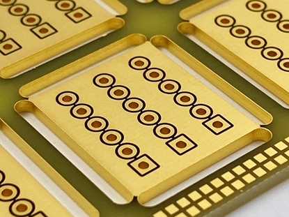
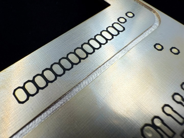
Plated slots in PCBs are often referred to as "long holes." These are either milled or nibbled during production. Nibbling refers to the drilling of many overlapping holes, resulting in a slot. For this process, a special nibbling drill with a specific grind is used. In both cases, the tool is subjected to higher stress—either from the horizontal movement during milling or from the continuous drilling along an edge, where the nibbling drill slides sideways along the hole's edge. Therefore, the smallest tool diameter that can be used for slots is 0.50 mm, as smaller tools would lack the necessary stability.
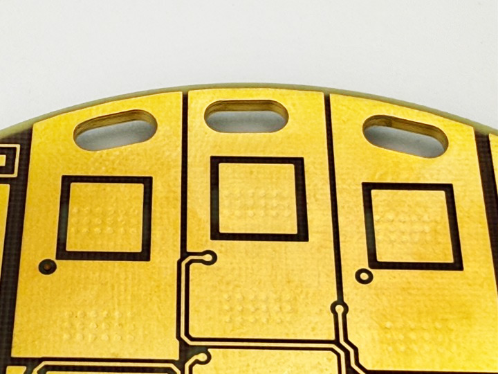
When preparing data, it is important to note that plated slots also require an annular ring. Standard annular rings are 0.20 mm all around. In special cases, this can be reduced to 0.15 mm.

After the electroplating process, a 0.50 mm milled slot will typically become about 0.45 to 0.40 mm wide, as the copper buildup reduces the slot width. This is the smallest possible plated slot. Common standard slot widths are 1.0 mm and 1.6 mm. Thinner plated slots may experience tool deviation or slight misalignment due to the forces acting on the tools. Additionally, it is very difficult to remove milling dust from very narrow slots before plating, which can result in minor over-plated burrs.
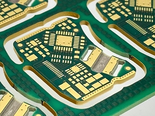
Plated milling areas refer to a much larger region than just a slot that is milled out of the PCB and plated. Depending on the size of this area, production can face certain challenges. In specific plating processes (e.g., panel plating), the laminate must cover these large areas without tearing. Pattern plating is more advantageous in such cases. It is also important to note that a milled edge does not achieve the usual roughness that is desirable for optimal adhesion in plated-through processes. The copper adhesion in plated milling areas is weaker than in plated holes. In multilayer boards, it is therefore essential to connect the inner layer copper to the plated milling areas to stabilize them.
In CAM processing, it is important to ensure that, as with plated contours, a sufficiently wide annular ring is provided.
Since these involve larger areas and the laminate adhesion can be critical depending on the process, we recommend 0.25 mm or significantly more if possible.
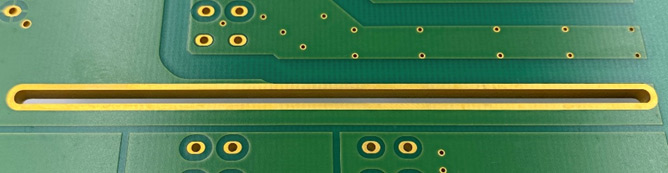
Plated contours on PCBs are usually created using a 2.00 mm or 2.40 mm milling tool. It is important to note that the PCB still requires connections to the manufacturing panel. Therefore, a fully plated contour around the entire edge is not possible. Corners are typically used for these connections. However, depending on the size and design, other connection points may also be necessary. Particularly when the PCBs are large and the plated milling cuts are long, additional hold points must be added to ensure that the panels do not become unstable during production. At these hold points, once the boards are separated, there will be no metallization on the PCB edge.
The aforementioned disadvantages regarding the adhesion of a plated contour also apply here, as milling leaves smoother edges compared to drilling. Therefore, it is also essential to connect any available inner layer copper to the plated contour wherever possible.
In CAM processing, it is important to ensure that an adequately wide annular ring is provided. This ring typically includes the entire 2.00 mm outer milling tool, meaning the copper must extend at least 2.25 mm beyond the future contour edge to ensure the plated contour milling tool runs entirely within the copper.
So-called half-opens represent a special type of plated outlines. Please refer to the dedicated section for more information.
Through-plated depth milling should be treated like standard depth milling in the CAM process, but only on one side, as it does not go through the entire circuit board.
As with any depth milling, either the milling depth or the remaining material thickness must be explicitly specified. Common tolerances for depth milling are +/- 0.20 mm. In some cases, more precise tolerances are possible (more expensive).
In multilayer boards with small layer spacing, it is important to ensure that the underlying inner layers have copper clearance within this depth tolerance, so that the through-plated depth milling does not cause a short circuit.
Plated slot contours and plated slots are specialized PCB machining features that provide various mechanical and functional benefits.
- Feature: Cutouts in PCBs that are plated with copper.
- Applications: Mechanical adjustments, connectors, cooling, and mounting purposes.
- Manufacturing Methods: Milling or laser processing, depending on material and precision requirements.
These features enhance the functionality and stability of the PCB.
- Precision: Plated slots help with accurate component positioning and prevent rotation.
- Stability: Improved mechanical durability of the PCB due to larger soldering areas.
- Ease of Assembly: Facilitates integration into enclosures or assemblies and sometimes prevents component rotation.
The machining process depends on the material and thickness of the PCB.
- Milling: A mechanical process suitable for high precision and wider plated slots.
- Laser Processing: Ideal for fine and complex contours or flexible PCBs.
- Hybrid Methods: Rare combinations of different techniques.
FR4 is optimal for plated slots and contours. Polyimides work well. Rogers is less suitable. Aluminum IMS is not possible.
- FR4: Standard PCB material with high stability for plated slots.
- Flexible Polyimide PCBs: Plated slots are possible but may crack under bending stress.
- Rogers: Plated slots can be manufactured, but adhesion is poor. Slots should be short, and plated contours should be avoided.
- Aluminum Substrates: Copper plating cannot be applied directly to aluminum.
In principle, any shape or "path" can be turned into a plated slot. They do not always have to be straight. Possible shapes include:
- Plated Slot: An internal, through-plated cut.
- Plated Contour: The outer contour of the PCB with copper plating.
- Plated Depth Milling: A partial-depth milling process with copper plating.
- Half-Opens or "Stamp Contour": A special form where plated holes on the edge are partially milled through.
Milled plated slots typically have a minimum width of 0.5 mm. For laser-cut flexible PCBs, the minimum final diameter is 0.2 mm.
- Mechanical Processing: Slots are usually milled or laser-cut 0.10 mm larger.
- Electroplating: Copper plating reduces the final slot size.
- Milling Tools: The smallest milling bits are usually ~1.0 mm; thinner bits break under horizontal stress, requiring nibbling instead.
- Nibbling Tools: The smallest nibbling cutters have a 0.6 mm diameter.
Very thin milling bits tend to deviate due to rotation forces, so nibbling is used instead.
- Nibbling: Creating a slot by overlapping multiple drilled holes. Pros: Suitable for smaller plated slot diameters down to 0.6 mm and results in straighter cuts. Cons: More expensive and sometimes less clean.
- Milling: Used for wider slots >1 mm. This is faster and more cost-effective.
Basic plated slots for components are included unless they are too narrow or used in large quantities.
- Plated contours: Edge plating is not included in online calculations.
- Half-open plated slots ("stamp contours") are highly complex and not included.
- Plated depth milling must be processed individually and requires a custom quote.

Elektronik-Design
- Expertise through active exchange
- Expertise through training and further education
- ISO 9001:2015 Quality Management
- ISO 14001:2015 Environmental Management

- UL for rigid FR4 PCBs
- UL for flexible circuit boards
- UL for aluminum IMS boards


