Hard gold | connctor gold | electrolytic gold
Hard- and connctor gold - kings of PCB surfaces
General Distinctions & Types
Hard gold is an electroplated gold coating that, thanks to cobalt doping, is significantly more resistant to mechanical wear. This makes it ideal for connectors, switches, or other contact surfaces that experience high mechanical stress.
In the past, hard gold layers of around 3 µm were not uncommon, which is considered an optimal thickness, as stability tends to decrease with thicker layers due to the risk of cracking. However, such thick layers are now rare, as gold prices have risen sharply, and in the fast-paced consumer market, especially for mass-produced items, wear cycles are often estimated to be shorter.
Typical hard gold thicknesses include:
- 0.3 µm: Low-cost hard gold for mass-market consumer products from Asia
- 0.5 - 0.8 µm: Standard for mass production and prototypes
- 1.2 µm: Maximum hard gold thickness achievable in Asian mass production
- 1 - 3 µm: For high-end prototypes and small series, Made in Germany
Important Note: The manufacturing effort for a PCB with hard gold increases significantly if the board is not to receive a solder mask. In this case, an additional cover layer must be applied to protect the areas that are not to be coated with hard gold.
Hard Gold Becomes Connector Gold
Connector gold is the most common use of hard gold. The term "connector gold" refers to hard gold plating applied to the edge of a PCB for a connector.
Simply put: Hard gold + chamfering = connector gold.
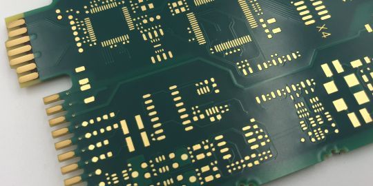
In the supplied data, it is only important that it is clear and defined whether and where connector gold is to be applied. The detailed processing of the data is handled by the PCB manufacturer during the CAM processing of the board.
Each individual pad of the connector receives a connector gold extension beyond the PCB outline, also called “plating bus”.
All of these are then connected with a wide trace.

In the panel, all of these wide traces are then connected to each other and routed beyond the panel outline. However, it is also possible to create multiple separate connector gold extensions, for example, if the top row of PCBs is rotated by 180°.
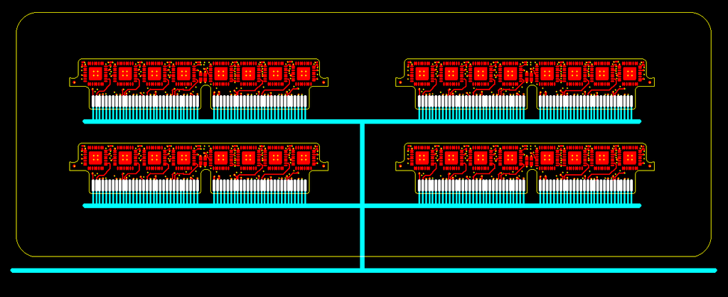
Now these wide traces are connected to the plating frame of the production panel. This allows all required pads to be electroplated with gold.
Chamfering
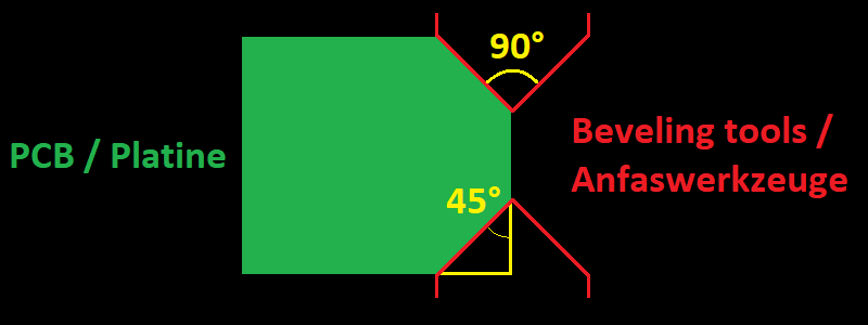
Connector edges on the PCB are often chamfered to facilitate easier insertion of the connector. A 90° chamfering tool is typically used for this purpose, resulting in a chamfer angle of 45°. However, especially in production in China, various other chamfering tools are available to achieve different angles.
Removal of Connector Gold Extensions
When milling the PCB, the connector gold extensions are milled through. As usual, milling through copper exposes bare copper and creates burrs, which can be problematic for certain applications.
Additionally, some layouts include connectors where not all pads are intentionally the same length. However, the connector gold extensions artificially lengthen all pads right up to the milling edge. This, too, can be problematic for certain applications.
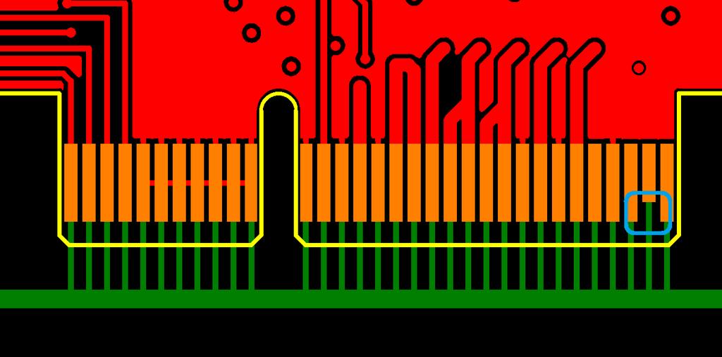
There is an option to remove the added connector gold extensions. Essentially, there are two methods available, one of which is only partially suitable.
Etch-back Process
In this method, the connector gold extensions are cleanly and precisely etched away (etched “back”) after the gold plating. This is a very accurate and high-quality process, but it is significantly more time-consuming and expensive than the Z-axis milling process.
Z-Axis Milling Process
In this method, the connector gold extensions are milled away after the gold plating. A Z-axis milling cut of approximately 0.10-0.15 mm is made into the PCB, directly along the pads.

Since this is a mechanical process, it is less accurate compared to etching the extensions. Furthermore, milling involves cutting through copper, which exposes bare copper and creates burrs. This process tends to be cheaper and allows for faster delivery times, but it comes with the aforementioned drawbacks.
Hard Gold on Non-Connector Pads
It is also possible to apply hard gold in the middle of the PCB. However, this is significantly more complicated, as connector gold extensions are still required via traces, and these must still come from outside the PCB and be routed to the pad. Typically, it is no longer referred to as "connector gold," as the application does not involve a classic plugging action.
To achieve hard gold in this area, the pads are connected through (multiple) inner layers and via (multiple) layer transitions.
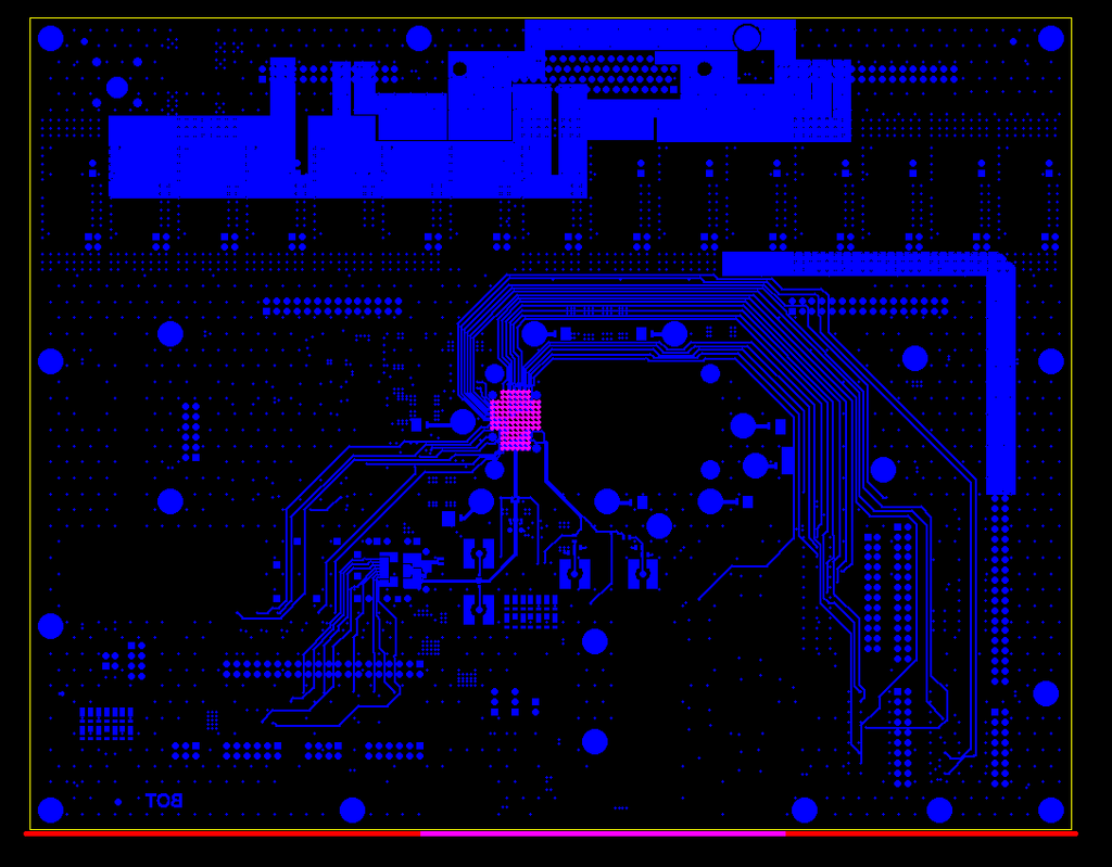
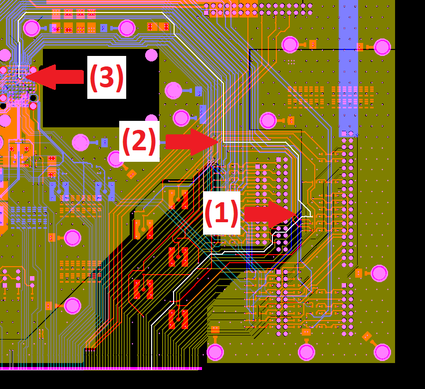
The relevant trace in the example shown below is highlighted in white. In this case, the galvanic connection is located on the inner layers.
First, a trace runs on IL3 up to (1).
(1) Here, this trace is connected via a via to a trace on the TOP layer.
(2) The trace on the TOP layer continues and is connected via a via to a trace on IL6.
(3) Here, the trace on IL6 ends and is connected via a via-in-pad to the pad on the BOTTOM layer.
In this way, all the pads shown (see image above) can be hard gold plated.
Advantages Over Chem. NiAu (ENIG)
Hard gold offers several advantages compared to chemical NiAu (immersion gold), making it particularly suitable for certain applications:
- Higher Abrasion Resistance: A hard gold coating is significantly more resistant to mechanical wear due to its special alloy compared to the chemically applied NiAu coating. This is especially beneficial in applications with frequent mating cycles, as hard gold remains intact longer and maintains contact quality.
- Stable Contact Resistance: Hard gold provides a more stable and lower contact resistance compared to chemical NiAu. The thicker and more robust gold layer ensures that conductivity remains consistent even with frequent use and under load, leading to more reliable signal transmission.


